Additive 3D nanofabrication for photonic integration
Facet-attached micro-lenses
Hybrid photonic integration combines complementary advantages of different material platforms, offering superior performance and flexibility compared with monolithic approaches. This applies in particular to multi-chip concepts, where components can be individually optimized and tested.
Up to now the assembly of such systems, however, requires expensive high-precision alignment and adaptation of optical mode profiles.
We show that these challenges can be overcome by in situ printing of facetattached beam-shaping elements. Our approach allows precise adaptation of vastly dissimilar mode profiles and permits alignment tolerances compatible with cost-efficient passive assembly techniques. We demonstrate a selection of beam-shaping elements at chip and fibre facets, achieving coupling efficiencies of up to 88% between edge-emitting lasers and single-mode fibres. We also realize printed free-form mirrors that simultaneously adapt beam shape and propagation direction, and we explore multi-lens systems for beam expansion. The concept paves the way to automated assembly of photonic multi-chip systems with unprecedented performance and versatility.
 © Philipp-Immanuel Dietrich
Vanguard Photonics’ collaborators at Karlsruhe Institute of Technology (KIT) have recently published these methods that allow to connect single-mode components using 3D-printed freeform optics in Nature Photonics see https://www.nature.com/articles/s41566-018-0133-4 to find out more.
The technology is commercialized by Vanguard Photonics GmbH. Take a look at our web-shop or contact us for further information.
Photonic wire bonding
Over the last decade, tremendous progress has been made in on-chip integration of photonic circuits driven by massive research investments of both industry and public institutions. However, packaging and assembly of photonic systems from discrete chips still represents a major technical and commercial challenge. In many cases, the lack of an industrially viable assembly technology hampers successful commercialization of photonic integrated systems, even though the fundamental chip-level building blocks would be available.
The fundamental problem behind this is that coupling of photonic chips is much more difficult than coupling of electronic chips: While in electronics, a simple conductive connection is sufficient to guide electrons from one chip to another, low-loss photonic connections require careful matching of mode field sizes and highly precise alignment of optical chips such that light exiting the output facet of one chip is directly coupled into the input facet of another chip. 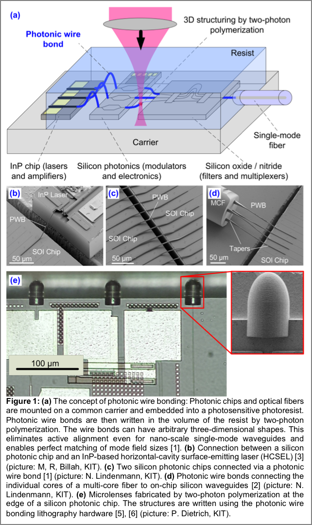 This is particularly challenging when it comes to semiconductor-based photonic chips carrying high-index contrast waveguides with mode field diameters of the order of 1 µm or less. Assembly of such systems requires so-called active alignment techniques, where the optical coupling efficiency is continuously monitored and optimized during the alignment process. These processes are slow and often involve expensive manual assembly. In addition, in case of chips with different mode field sizes, additional elements such as micro-lenses are needed, which further complicates system assembly.
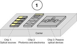
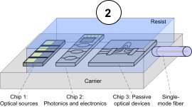
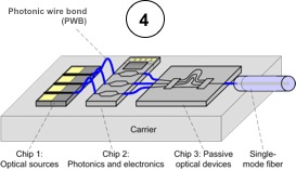
Vanguard’s proprietary approach promises to overcome these limitations by in-situ structuring of photonic waveguides and micro-optical components using high-end additive 3D nanofabrication techniques. This leads to the concept of photonic wire bonding, which can be considered as the optical analogue to metal wire bonding in electronics. Photonic wire bonds (PWB) are single-mode freeform waveguides that efficiently connect integrated optical chips to each other or to optical fibers, see Figure 1. Our research partners at KIT have demonstrated that photonic wire boinds can connect to a wide variety of on-chip waveguides and optical fibers, see Figure 1 (b), (c), and (d) [1] – [4]. For chip-to-chip connections, Figure 1 (b), lateral dimensions of PWB waveguides typically amount to 1…2 µm, and the pitch can be smaller than 5 µm, enabling hundreds of PWB per millimeter of chip edge [1]. For a connection of two silicon-on-insulator (SOI) waveguides, insertion losses of 1 dB … 2 dB have been demonstrated with negligible variation in the wavelength range 1200 nm … 1600 nm [1]. Similar loss figures are obtained when connecting PWB to multi-core fibers (MCF) [2] or to InP-based laser sources [3], [4].
Fabrication of Photonic Wire Bonds
Photonic wire bonds are fabricated in several steps using direct-write 3D laser lithography based on two-photon polymerization [1].
 Step 1
Photonic chips and fibers are fixed to a common submount using standard pick-and-place machinery with moderate precision.
Step 2
The interconnect regions are then embedded into a photosensitive resist, and the actual positions of waveguide facets and coupling structures within the resist are detected using 3D machine vision techniques with sub-100 nm accuracy.
 Step 3

The shape of the photonic wire bond (PWB) waveguide is designed according to the recorded facet positions and defined using two-photon lithography.
 Step 4
Unexposed resist material is removed in a development step, and the structures are finally embedded in a low-index cladding material.
Since the shape of the bonds is adapted to the positions of the coupling interfaces, high-precision alignment of the optical chips becomes obsolete. Moreover, by using tapered freeform waveguides, photonic wire bonding can cope with vastly different mode fields of the devices to be connected. The technique can be fully automated and is well suited for high-throughput mass production.
References
- [1] Lindenmann, N.; Balthasar, G.; Hillerkuss, D.; Schmogrow, R.; Jordan, M.; Leuthold, J.; Freude, W.; Koos, C.: ‘Photonic wire bonding: a novel concept for chip-scale interconnects’; Opt. Express 20, 17667-17677, (2012)
- [2] Lindenmann, N.; Dottermusch, S.; Goedecke, M.-L.; Hoose, T.; Billah, M.-R.; Onanuga, T.-P; Hofmann, A.; Freude, W.; Koos, C.: ‘Connecting silicon photonic circuits to multicore fibers by photonic wire bonding’; Journal of Lightwave Technology 33, 755 – 760 (2015)
- [3] Billah, M. R.; Hoose, T.; Onanuga, T.; Lindenmann, N.; Dietrich, P.; Wingert, T.; Goedecke, M. L.; Hoffmann, A.; Troppenz, U.; Sigmund, A.; Möhrle, M.; Freude, W.; Koos, C.: ‘Multi-chip integration of lasers and silicon photonics by photonic wire bonding’, Conf. on Lasers and Electro-Optics (CLEO’15), San Jose (CA), USA, May 10–15, 2015. Paper STu2F.
- [4] Hoose, T.; Billah, M.; Blaicher, M.; Marin, P.; Dietrich, P.-I.; Hofmann, A.; Troppenz, U.; Moehrle, M.; Lindenmann, N.; Thiel, M.; Simon, P.; Hoffmann, J.; Goedecke, M.-L-.; Freude, W.; Koos. C.: ’Multi-Chip Integration by Photonic Wire Bonding: Connecting Surface and Edge Emitting Lasers to Silicon Chips’, Optical Fiber Communication Conference (OFC’16), Anaheim (CA), USA, 20 – 24 March, 2016
- [5] Schneider, S.; Lauermann, M.; Dietrich, P.-I.; Weimann, C.; Freude, W.; Koos, C.: “Optical coherence tomography system mass-producible on a silicon chip”; Express 24, 1573-1586 (2016)
- [6] Dietrich, P.; Reuter, I.; Blaicher, M.; Schneider, S.; Billah, M. R.; Hoose, T.; Hofmann, A.; Caer, C.; Dangel, R.; Offrein, B.; Moehrle, M.; Troppenz, U.; Zander, M.; Freude, W.; Koos, C.: ‘Lenses for low-loss chip-to-fiber and fiber-to-fiber coupling fabricated by 3D direct-write lithography’, Conf. on Lasers and Electro-Optics (CLEO’16), San Jose (CA), USA, June 5–10, 2016. Paper SM1G.4