by Alois Hauk | Sep 16, 2016 |
3D nanoprinting of free-form coupling elements for hybrid photonic integration
Hybrid photonic integration combines complementary advantages of different material platforms, offering superior performance and flexibility compared with monolithic approaches. This applies in particular to multi-chip concepts, where components can be individually optimized and tested.
Up to now the assembly of such systems, however, requires expensive high-precision alignment and adaptation of optical mode profiles.
We show that these challenges can be overcome by in situ printing of facetattached beam-shaping elements. Our approach allows precise adaptation of vastly dissimilar mode profiles and permits alignment tolerances compatible with cost-efficient passive assembly techniques. We demonstrate a selection of beam-shaping elements at chip and fibre facets, achieving coupling efficiencies of up to 88% between edge-emitting lasers and single-mode fibres. We also realize printed free-form mirrors that simultaneously adapt beam shape and propagation direction, and we explore multi-lens systems for beam expansion. The concept paves the way to automated assembly of photonic multi-chip systems with unprecedented performance and versatility.
 Vanguard Photonics’ collaborators at Karlsruhe Institute of Technology (KIT) have recently published these methods that allow to connect single-mode components using 3D-printed freeform optics in Nature Photonics see https://www.nature.com/articles/s41566-018-0133-4 to find out more.
The technology is commercialized by Vanguard Photonics GmbH. Take a look at our web-shop or contact us for further information.
© Philipp-Immanuel Dietrich
Printed micro-optics
 Photonic designers are creative folks and continuously come up with new ideas. Why slow this down by long prototyping cycles?
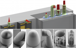
We can print a wide variety of customized or custom-designed micro-optical elements such as lensed fibre arrays, micro-lenses and free-form elements with sub-micrometer accuracy – on chip surfaces, laser facets, and optical fibers.
Micro-lenses fabricated by two-photon polymerization at the edge of a silicon photonic chip [see References 5, 6] (Picture: P. Dietrich, KIT)
by p373089 | Sep 1, 2016 |
Are you looking for flexible photonic system concepts that can address strongly heterogeneous markets based on a uniform technology?
 Vanguard’s multi-chip integration platform combines the technological flexibility of discrete systems with the compactness and economic advantages of large-scale photonic integration
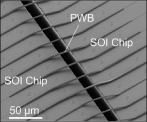
Two silicon on insulator (SOI) chips connected via free-form photonic wire bonds (PWB) to form a multi-chip-module [see References 1]. (Picture: N. Lindenmann, KIT)
by p373089 | Sep 1, 2016 |
High-speed communication systems cannot afford compromises – neither in performance, nor in price. Vanguard’s proprietary photonic wirebonding technology allows to merge the specific strengths of different photonic integration platforms in a hybrid multi-chip system. Connecting InP lasers to silicon photonic chips, to low index-contrast planar lightwave circuits (PLC), or to optical fibers is one of our favourite challenges.
You  think this can be useful in realizing the next generation of photonic engines for 400G Ethernet, data-center interconnects, or optical access networks? We are happy to help you find out!
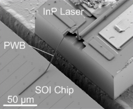
Connection between a silicon photonic chip and an InP-based horizontal-cavity surface-emitting laser (HCSEL) [see References 3] (Picture: M. R. Billah, KIT)
by p373089 | Sep 1, 2016 |
Industrial sensors must be reliable and robust – strong arguments for photonic integration. Do not let optical assembly and packaging challenges spoil the dream!
 Vanguard’s proprietary photonic wire bonding technology enables highly stable chip-scale photonic modules that can be fabricated at low cost. We are happy to try this out with you.
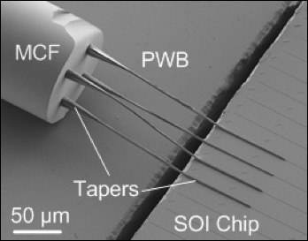
Photonic wire bonds (PWB) connecting the individual cores of a multi-core fiber (MCF) to on-chip silicon waveguides. [see References 2] (Picture: N. Lindenmann, KIT)
by p373089 | Sep 1, 2016 |
Let’s face it: There is simply no perfect integration platform for photonic systems! Instead, designers have to deal with a variety of material systems – silicon photonics, indium phosphide, TriPleX™, just to name a few.
Vanguard’s proprietary photonic wirebonding technology can merge the distinct advantages of these platforms by connecting single-mode photonic circuits across waveguide boundaries – without active alignment, and without additional elements for mode field adaptation.
Vanguard’s proprietary photonic wirebonding technology can merge the distinct advantages of these platforms by connecting single-mode photonic circuits across waveguide boundaries – without active alignment, and without additional elements for mode field adaptation.
Multi-chip module enabled by photonic wire bonding (PWB)
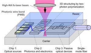 Photonic chips and optical fibers are mounted on a common carrier and embedded into a photosensitive photoresist. Photonic wire bonds are then written in the volume of the resist by two-photon polymerization. The wire bonds can have arbitrary three-dimensional shapes. This eliminates active alignment even for nano-scale single-mode waveguides and enables perfect matching of mode field sizes. [Picture see References 1-4]
 Vanguard Photonics’ collaborators at Karlsruhe Institute of Technology (KIT) have recently published these methods that allow to connect single-mode components using 3D-printed freeform optics in Nature Photonics see https://www.nature.com/articles/s41566-018-0133-4 to find out more.
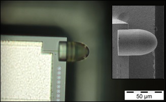 Photonic designers are creative folks and continuously come up with new ideas. Why slow this down by long prototyping cycles?