by p373089 | Sep 1, 2016 |
Are you looking for flexible photonic system concepts that can address strongly heterogeneous markets based on a uniform technology?
 Vanguard’s multi-chip integration platform combines the technological flexibility of discrete systems with the compactness and economic advantages of large-scale photonic integration
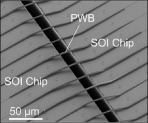
Two silicon on insulator (SOI) chips connected via free-form photonic wire bonds (PWB) to form a multi-chip-module [see References 1]. (Picture: N. Lindenmann, KIT)
by p373089 | Sep 1, 2016 |
Industrial sensors must be reliable and robust – strong arguments for photonic integration. Do not let optical assembly and packaging challenges spoil the dream!
 Vanguard’s proprietary photonic wire bonding technology enables highly stable chip-scale photonic modules that can be fabricated at low cost. We are happy to try this out with you.
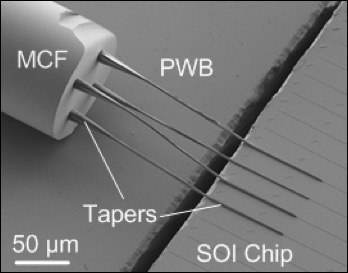
Photonic wire bonds (PWB) connecting the individual cores of a multi-core fiber (MCF) to on-chip silicon waveguides. [see References 2] (Picture: N. Lindenmann, KIT)
by p373089 | Sep 1, 2016 |
Let’s face it: There is simply no perfect integration platform for photonic systems! Instead, designers have to deal with a variety of material systems – silicon photonics, indium phosphide, TriPleX™, just to name a few.
Vanguard’s proprietary photonic wirebonding technology can merge the distinct advantages of these platforms by connecting single-mode photonic circuits across waveguide boundaries – without active alignment, and without additional elements for mode field adaptation.
Vanguard’s proprietary photonic wirebonding technology can merge the distinct advantages of these platforms by connecting single-mode photonic circuits across waveguide boundaries – without active alignment, and without additional elements for mode field adaptation.
Multi-chip module enabled by photonic wire bonding (PWB)
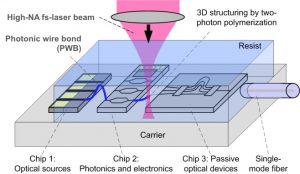 Photonic chips and optical fibers are mounted on a common carrier and embedded into a photosensitive photoresist. Photonic wire bonds are then written in the volume of the resist by two-photon polymerization. The wire bonds can have arbitrary three-dimensional shapes. This eliminates active alignment even for nano-scale single-mode waveguides and enables perfect matching of mode field sizes. [Picture see References 1-4]
 Vanguard’s multi-chip integration platform combines the technological flexibility of discrete systems with the compactness and economic advantages of large-scale photonic integration